2003 May 13 3
NXP Semiconductors
Product data sheet
High voltage double diode BAW101S
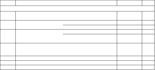
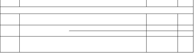
LIMITING VALUES
In accordance with the Absolute Maximum Rating System (IEC
60134).
Note
1. Device mounted on an FR4 printed-circuit board, cathode-lead mounting pad=
1
cm2.
ELECTRICAL CHARACTERISTICS
Tj
=
25
°C unless otherwise specified.
Note
1. Pulse test: pulse width
=
300
μs; δ
=
0.02.
SYMBOL
PARAMETER
CONDITIONS
MIN.
MAX.
UNIT
Per diode
VR
continuous reverse voltage
?
300
V
series connection
?
600
V
VRRM
repetitive peak reverse voltage
?
300
V
series connection
?
600
V
IF
continuous forward current
single diode loaded; note
1; see
Fig.2
?
250
mA
double diode loaded; note
1; see
Fig.2
?
140
mA
IFRM
repetitive peak forward current
?
625
mA
IFSM
non-repetitive peak forward
current
square wave; Tj
=
25
°C prior to surge;
t
=
1
μs
?
4.5
A
Ptot
total power dissipation
Tamb
=
25
°C; note
1
?
350
mW
Tstg
storage temperature
?65
+150
°C
Tj
junction temperature
?
150
°C
Tamb
operating ambient temperature
?65
+150
°C
SYMBOL
PARAMETER
CONDITIONS
MIN.
MAX.
UNIT
Per diode
VBR(R)
reverse breakdown voltage
IR
=
100
μA
300
?
V
VF
forward voltage
IF
=
100
mA; note
1
?
1.1
V
IR
reverse current
VR
=
250
V
?
150
nA
VR
=
250
V; Tamb
=
150
°C
?
50
μA
trr
reverse recovery time
when switched from IF
=
30
mA to IR
=
30
mA;
?
RL
=
100
?; measured at IR
=
3
mA
50
ns
Cd
diode capacitance
VR
=
0
V; f
=
1
MHz
?
2
pF


发布紧急采购,3分钟左右您将得到回复。
相关PDF资料
BAW101S-7
DIODE ARRAY 300V 250MA SOT363
BAW101V-7
DIODE ARRAY 325V 250MA SOT563
BAW156,215
DIODE DUAL 75V 160MA SOT-23
BAW156-F
DIODE SWITCH 85V 250MW SOT23-3
BAW56-7
DIODE DUAL SW 75V 350MW SOT23-3
BAW567DW-7
DIODE ARRAY QUAD SW 200MW SC70-6
BAW56DW-7
DIODE ARRAY QUAD SW 75V SC70-6
BAW56LT1G
DIODE SWITCH DUAL CA 70V SOT23
相关代理商/技术参数
BAW101S-7
功能描述:二极管 - 通用,功率,开关 HIGH VOLT DUAL 50ns 300V 150nA Switching RoHS:否 制造商:STMicroelectronics 产品:Switching Diodes 峰值反向电压:600 V 正向连续电流:200 A 最大浪涌电流:800 A 配置: 恢复时间:2000 ns 正向电压下降:1.25 V 最大反向漏泄电流:300 uA 最大功率耗散: 工作温度范围: 安装风格:SMD/SMT 封装 / 箱体:ISOTOP 封装:Tube
BAW101V
制造商:DIODES 制造商全称:Diodes Incorporated 功能描述:HIGH VOLTAGE DUAL SWITCHING DIODE
BAW101V-7
功能描述:二极管 - 通用,功率,开关 HV DUAL SW DIODE 300V RoHS:否 制造商:STMicroelectronics 产品:Switching Diodes 峰值反向电压:600 V 正向连续电流:200 A 最大浪涌电流:800 A 配置: 恢复时间:2000 ns 正向电压下降:1.25 V 最大反向漏泄电流:300 uA 最大功率耗散: 工作温度范围: 安装风格:SMD/SMT 封装 / 箱体:ISOTOP 封装:Tube
BAW156
功能描述:DIODE SWITCH 250MW 85V SOT23-3 RoHS:否 类别:分离式半导体产品 >> 二极管,整流器 - 阵列 系列:- 其它有关文件:STTH10LCD06C View All Specifications 标准包装:1,000 系列:- 电压 - 在 If 时为正向 (Vf)(最大):2V @ 5A 电流 - 在 Vr 时反向漏电:1µA @ 600V 电流 - 平均整流 (Io)(每个二极管):5A 电压 - (Vr)(最大):600V 反向恢复时间(trr):50ns 二极管类型:标准 速度:快速恢复 = 200mA(Io) 二极管配置:1 对共阴极 安装类型:表面贴装 封装/外壳:TO-263-3,D²Pak(2 引线+接片),TO-263AB 供应商设备封装:D2PAK 包装:带卷 (TR) 产品目录页面:1553 (CN2011-ZH PDF) 其它名称:497-10107-2
BAW156 _R1 _00001
制造商:PanJit Touch Screens 功能描述:
BAW156 T/R
功能描述:整流器 DIODE LOW LEAKAGE TAPE-7 RoHS:否 制造商:Vishay Semiconductors 产品:Standard Recovery Rectifiers 配置: 反向电压:100 V 正向电压下降: 恢复时间:1.2 us 正向连续电流:2 A 最大浪涌电流:35 A 反向电流 IR:5 uA 安装风格:SMD/SMT 封装 / 箱体:DO-221AC 封装:Reel
BAW156,215
功能描述:整流器 DIODE LOW LEAKAGE RoHS:否 制造商:Vishay Semiconductors 产品:Standard Recovery Rectifiers 配置: 反向电压:100 V 正向电压下降: 恢复时间:1.2 us 正向连续电流:2 A 最大浪涌电流:35 A 反向电流 IR:5 uA 安装风格:SMD/SMT 封装 / 箱体:DO-221AC 封装:Reel
BAW156/ZLR
功能描述:DIODE ARRAY GEN PURP 75V SOT23 制造商:nxp usa inc. 系列:- 包装:带卷(TR) 零件状态:停產 二极管配置:1 对共阳极 二极管类型:标准 电压 - DC 反向(Vr)(最大值):75V 电流 - 平均整流(Io)(每二极管):160mA(DC) 不同 If 时的电压 - 正向(Vf:1.25V @ 150mA 速度:小信号 =< 200mA(Io),任意速度 反向恢复时间(trr):3μs 不同?Vr 时的电流 - 反向漏电流:5nA @ 75V 工作温度 - 结:150°C(最大) 安装类型:表面贴装 封装/外壳:TO-236-3,SC-59,SOT-23-3 供应商器件封装:TO-236AB(SOT23) 标准包装:3,000
